What Is An Electrical Conductor Fundamentals Applications
Table of Contents
- Definition and Core Characteristics of Electrical Conductors
- Atomic Structure and Electron Mobility in Conductors vs. Insulators
- Common Electrical Conductor Materials and Their Properties
- Factors Influencing Conductivity Beyond Material Composition
- Mechanisms of Electrical Conductivity
- Quantum Mechanical Principles Governing Electron Transport
- Temperature Dependence of Resistivity and Conductivity
- Impact of Impurities on Conductivity in Metals vs. Alloys
- Drift Velocity, Mean Free Path, and Relaxation Time in Conductors
- Practical Applications and Engineering Uses of Electrical Conductors
- Selection Criteria for Conductors in High-Voltage Transmission Lines
- Performance Comparison: Superconductors vs. Traditional Conductors
- Case Studies: Conductor Material Choices and System Reliability
- Safety and Environmental Considerations in Electrical Conductor Applications
- Common Hazards Associated with Poor Conductor Selection and Mitigation Strategies
- Environmental Impact of Conductor Material Extraction and Sustainable Alternatives
- Safety Protocols for Handling High-Conductivity Materials in Laboratories and Manufacturing
- Emerging Technologies and Innovations in Electrical Conductors
- Nanomaterials in Conductive Applications
- Topological Insulators: Surface Conductivity vs. Bulk Insulation
- Conductive Inks and Polymers for Printed Electronics
- Timeline of Key Milestones in Conductor Technology
- Experimental Methods and Measurements in Electrical Conductivity
- Four-Point Probe Method for Conductivity Measurement
- Constructing a Simple Conductivity Experiment with Household Items
- Eddy Current Testing for Non-Destructive Evaluation of Conductors
- FAQ
- What is the definition of an electrical conductor?
- How do electrical conductors differ from electrical insulators?
- Can you give examples of electrical conductors?
- What is an electronic conductor?
- What exactly is an electrical wire?
- How is electrical conductivity defined?
Electrical conductors form the backbone of modern electrical systems, enabling the efficient transfer of energy through the controlled movement of electrons. From power grids spanning continents to the intricate circuitry within smartphones, these materials underpin nearly every technological advancement in the 21st century. Understanding their atomic structure, conductivity mechanisms, and practical limitations is essential for engineers, physicists, and technicians designing systems that balance performance, safety, and sustainability.
At its core, an electrical conductor distinguishes itself through its ability to permit electron flow with minimal resistance, a property dictated by its atomic configuration—particularly the presence of free or loosely bound electrons. This fundamental characteristic contrasts sharply with insulators, where tightly bound electrons create a substantial energy barrier, or band gap, preventing current. The choice of conductor material, whether copper for its cost-effectiveness or silver for its superior conductivity, directly influences system efficiency, durability, and environmental impact. As industries increasingly demand lighter, more efficient, and sustainable solutions, innovations in nanomaterials and superconductors are redefining the boundaries of what conductors can achieve.

Definition and Core Characteristics of Electrical Conductors
Electrical conductors are materials that allow the free movement of electric charge, primarily electrons, enabling efficient current flow in electrical circuits. Their fundamental role stems from their atomic structure, which facilitates electron mobility through delocalized or loosely bound electrons. This property distinguishes conductors from insulators, where electron movement is restricted due to tightly bound atomic structures. The effectiveness of a conductor is quantified by its electrical resistivity (ρ), measured in ohm-meters (Ω·m), and its conductivity (σ), the reciprocal of resistivity, expressed in siemens per meter (S/m). Lower resistivity indicates higher conductivity, making the material more suitable for applications requiring minimal energy loss.
Conductivity arises from the presence of free or conduction electrons in a material’s atomic lattice. In metals, these electrons occupy partially filled energy bands, allowing them to move freely under an applied electric field. In contrast, insulators possess a large band gap between their valence and conduction bands, preventing electron excitation and current flow. Semiconductors occupy an intermediate state, with band gaps small enough to allow controlled conductivity under specific conditions (e.g., doping or thermal excitation).
Atomic Structure and Electron Mobility in Conductors vs. Insulators
The distinction between conductors and insulators is rooted in their electronic band structures, which determine how electrons interact with atomic nuclei. In conductors, particularly metals, the outermost electron shells (valence electrons) are not tightly bound to individual atoms. Instead, they form a "sea of electrons" that moves collectively through the lattice, responding to external electric fields. This phenomenon is described by the Drude model and Fermi-Dirac statistics, which explain electron behavior in metals at thermal equilibrium.Key Atomic Properties:Insulators, by contrast, exhibit a wide band gap (typically > 4 eV), where electrons require significant energy to transition from the valence band to the conduction band. Common insulators like ceramics or polymers have fully occupied valence bands and empty conduction bands at standard temperatures, preventing electron movement. Semiconductors, such as silicon or germanium, have smaller band gaps (0.1–4 eV), allowing conductivity under conditions like doping or temperature increases.
Metallic Bonding: Valence electrons are delocalized across the lattice, enabling high electron mobility. Band Overlap: In metals, the valence band and conduction band overlap, allowing continuous electron flow. Low Ionization Energy: Easier removal of electrons from atoms, reducing resistance to current.
Common Electrical Conductor Materials and Their Properties
The selection of conductor materials depends on factors such as resistivity, thermal conductivity, cost, and mechanical strength. Below is a structured comparison of widely used conductor materials, emphasizing their atomic properties and practical applications.Resistivity (ρ) and Conductivity (σ) Relationship:The following table summarizes key conductor materials, their resistivity, thermal conductivity, and typical applications:
\[
\sigma = \frac{1}{\rho}
\]
Lower ρ values (e.g., silver at 1.59 × 10⁻⁸ Ω·m) indicate superior conductivity.
| Material | Resistivity (Ω·m at 20°C) | Thermal Conductivity (W/m·K) | Typical Applications |
|---|---|---|---|
| Silver (Ag) | 1.59 × 10⁻⁸ | 429 | High-frequency circuits, electrical contacts, superconducting alloys (when alloyed) |
| Copper (Cu) | 1.68 × 10⁻⁸ | 401 | Power transmission cables, wiring, PCB traces, motor windings |
| Gold (Au) | 2.44 × 10⁻⁸ | 318 | Electrical connectors, corrosion-resistant coatings, aerospace wiring |
| Aluminum (Al) | 2.65 × 10⁻⁸ | 237 | Overhead power lines, aircraft wiring, heat sinks |
| Copper-Nickel Alloys (e.g., CuNi10) | 2.0–3.0 × 10⁻⁷ | 20–50 | Marine cables, corrosion-resistant piping, chemical processing |
| Graphite (Carbon) | 3.5–60 × 10⁻⁶ (anisotropic) | 120–160 (in-plane) | Electrodes, brushes in electric motors, conductive coatings |
| Tungsten (W) | 5.65 × 10⁻⁸ | 174 | Filaments in incandescent bulbs, X-ray tubes, high-temperature applications |
Factors Influencing Conductivity Beyond Material Composition
While intrinsic material properties dominate conductivity, external factors such as temperature, impurities, and mechanical stress significantly alter performance. Understanding these variables is critical for optimizing conductor applications.Temperature Dependence of Resistivity:Key Influences:
\[
\rho(T) = \rho_0 [1 + \alpha (T - T_0)]
\]
where:
\(\rho_0\) = resistivity at reference temperature \(T_0\), \(\alpha\) = temperature coefficient of resistivity (positive for metals, negative for semiconductors).
Practical Example:
In power transmission, aluminum conductors are often used in overhead lines due to their lightweight, but their higher resistivity necessitates larger cross-sectional areas compared to copper for equivalent current capacity. Copper remains dominant in low-voltage applications (e.g., household wiring) despite its cost due to superior conductivity and ductility.
Mechanisms of Electrical Conductivity
Electrical conductivity in materials arises from the collective behavior of free electrons under the influence of an electric field, governed by quantum mechanical principles and thermodynamic interactions. The movement of charge carriers—primarily electrons in metals—is not random but follows probabilistic distributions influenced by energy states, lattice vibrations, and impurities. Understanding these mechanisms requires examining the Fermi-Dirac statistics that dictate electron distribution, the role of electron mobility in response to external fields, and how thermal and structural factors modify resistance. This section explores the quantum foundations of conductivity, the mathematical relationships between temperature, resistivity, and conductivity, and the impact of impurities on electron transport in metals and alloys.
Quantum Mechanical Principles Governing Electron Transport
The conduction process in metals is fundamentally described by band theory, where electrons occupy energy states within a conduction band separated from a valence band by a negligible energy gap. At absolute zero, electrons fill states up to the Fermi level (EF), the highest occupied energy level at equilibrium. When an electric field is applied, electrons near the Fermi level gain energy and transition to higher states, enabling net current flow. Key quantum parameters include:
- Fermi Level (EF): Defined by the equation for free electrons in a metal:
\( E_F = \frac{\hbar^2}{2m} (3\pi^2 N/V)^{2/3} \),In copper, \( E_F \approx 7.0 \) eV, reflecting its high conductivity due to a dense electron sea at the Fermi surface.
where \( \hbar \) is the reduced Planck constant, \( m \) is electron mass, \( N \) is electron count, and \( V \) is volume.
- Electron Mobility (\( \mu \)): Quantifies how readily electrons accelerate under an electric field (\( E \)), defined as:
\( \mu = \frac{v_d}{E} \),Mobility is inversely proportional to resistivity (\( \rho \)) via \( \sigma = n e \mu \), where \( \sigma \) is conductivity, \( n \) is carrier density, and \( e \) is electron charge. Copper’s mobility (\( \mu \approx 3.2 \times 10^{-3} \, \text{m}^2/\text{V}\cdot\text{s} \)) exceeds that of gold (\( \mu \approx 2.2 \times 10^{-3} \, \text{m}^2/\text{V}\cdot\text{s} \)) due to stronger electron-phonon scattering in gold.
where \( v_d \) is the drift velocity of electrons.
Temperature Dependence of Resistivity and Conductivity
Resistivity (\( \rho \)) in metals increases with temperature due to electron-phonon scattering, where lattice vibrations (phonons) impede electron flow. The empirical relationship is given by:\( \rho(T) = \rho_0 [1 + \alpha (T - T_0)] \),For copper, \( \alpha \approx 0.0039 \, \text{°C}^{-1} \), while for gold, \( \alpha \approx 0.0034 \, \text{°C}^{-1} \). This linear approximation holds for small temperature ranges but fails at cryogenic temperatures, where quantum scattering dominates.
where:
\( \rho_0 \) = resistivity at reference temperature \( T_0 \) (typically 20°C), \( \alpha \) = temperature coefficient of resistivity (TCR), specific to the material.
Key Observations:
Impact of Impurities on Conductivity in Metals vs. Alloys
Impurities disrupt the periodic potential of a crystal lattice, introducing scattering centers that reduce electron mean free path. The effect differs between metals (pure elements) and alloys (solid solutions of metals):Step-by-Step Mechanism in Metals:
1. Doping in Semiconductors (Analogous to Alloying):
where \( \rho_{imp} \) is temperature-independent. 2. Alloying in Metals:
Comparison Table: Impurity Effects in Metals vs. Alloys
| Parameter | Pure Metals | Alloys |
|---|---|---|
| Primary Scattering Source | Phonons (thermal) | Impurities + phonons |
| Temperature Dependence of \( \rho_{imp} \) | N/A (negligible) | Constant (independent of \( T \)) |
| Example | Copper (99.99% purity) | Bronze (Cu-Sn alloy) |
| Conductivity Impact | Maximized at low \( T \) | Reduced due to alloy scattering |
Drift Velocity, Mean Free Path, and Relaxation Time in Conductors
The drift velocity (\( v_d \)) of electrons under an electric field (\( E \)) is derived from the balance between acceleration and scattering events. Key parameters include:Drift Velocity:
\( v_d = -\mu E \),
where \( \mu = \frac{e \tau}{m} \), \( \tau \) is the relaxation time (average time between collisions).
Mean Free Path (\( \lambda \)):Material-Specific Examples:
\( \lambda = v_F \tau \),
where \( v_F \) is the Fermi velocity (~1.6 × 10⁶ m/s in copper).
Relaxation Time (\( \tau \)):
Visualization of Electron Dynamics:
Imagine electrons in copper as a fluid moving at \( v_F \) in random directions.
Practical Applications and Engineering Uses of Electrical Conductors
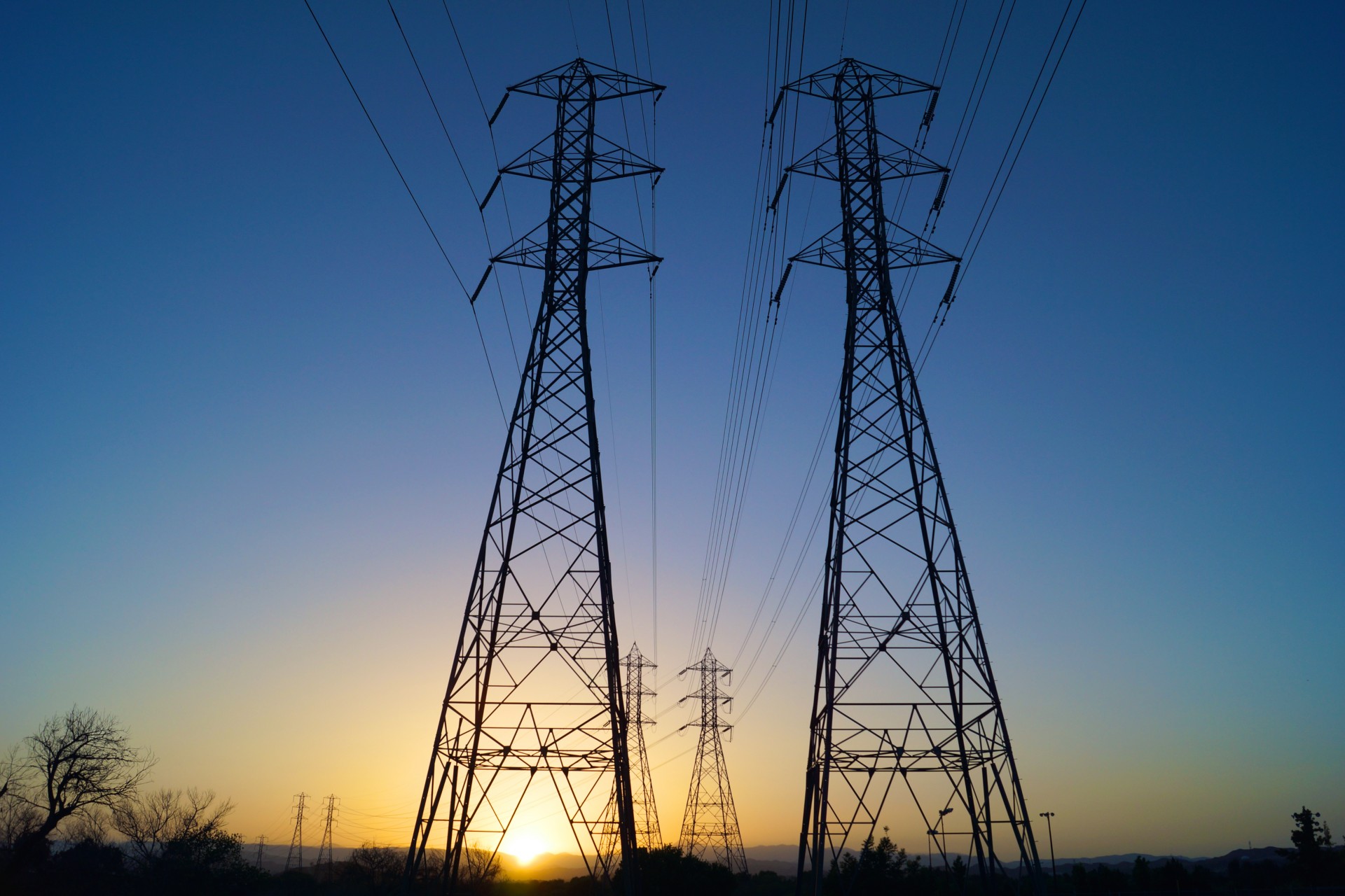
Electrical conductors form the backbone of modern infrastructure, enabling efficient power transmission, data communication, and industrial automation. Their selection in engineering applications depends on balancing material properties, environmental constraints, and operational demands. High-voltage transmission, superconducting technologies, and specialized systems such as aircraft wiring demonstrate how conductor choices directly influence system performance, reliability, and economic viability. This section explores the trade-offs in conductor selection, comparative performance of advanced materials, and real-world case studies where material decisions shaped critical systems.Selection Criteria for Conductors in High-Voltage Transmission Lines
High-voltage transmission lines require conductors that minimize energy loss while optimizing cost, weight, and mechanical strength. The primary selection criteria include electrical conductivity, tensile strength, corrosion resistance, and thermal performance. Copper and aluminum dominate this sector due to their balance of properties, but trade-offs exist between cost, weight, and efficiency.Key Trade-Offs in Conductor Selection:
Cost vs. Performance: Copper offers superior conductivity (~5.96 × 10⁷ S/m) but is significantly heavier and more expensive than aluminum (~3.78 × 10⁷ S/m). Aluminum conductors (e.g., ACSR—Aluminum Conductor Steel Reinforced) reduce costs by up to 60% while maintaining adequate conductivity for long-distance transmission. Weight vs. Mechanical Strength: Overhead transmission lines must support their own weight and environmental loads (e.g., ice, wind). Steel-core conductors (e.g., ACSR) combine aluminum’s conductivity with steel’s high tensile strength (~1,600 MPa for steel vs. ~200 MPa for aluminum), enabling longer spans and reduced tower structures. Thermal and Corrosion Resistance: Conductors in tropical or coastal regions require corrosion-resistant coatings (e.g., zinc or aluminum alloys) or materials like copper-clad steel to prevent degradation. Thermal expansion coefficients must also align with insulators to avoid sagging under high temperatures.
-
Electrical Efficiency:
High-voltage lines prioritize low resistivity to reduce I²R losses (Joule heating). For example, a 765 kV transmission line using copper may lose ~0.5% of power per 100 km, whereas aluminum increases losses to ~0.8% due to higher resistivity. However, aluminum’s lighter weight allows for larger cross-sectional areas (e.g., 1,270 kcmil vs. 750 kcmil for copper), compensating for losses in long-distance applications. -
Economic Viability:
Aluminum’s lower material cost (~$2,200/ton vs. ~$9,000/ton for copper) makes it preferable for projects with budget constraints. However, copper’s durability in high-stress environments (e.g., urban areas with frequent short circuits) justifies its use in substations and short-distance lines. -
Environmental and Installation Factors:
Conductors for remote or rugged terrains (e.g., mountainous regions) may use composite core conductors (e.g., aluminum with carbon fiber) to reduce weight without sacrificing strength. In urban settings, underground cables (e.g., XLPE-insulated copper) are chosen for safety and aesthetics, despite higher installation costs.
Industry Standards and Design Guidelines:
IEEE Std 738 provides guidelines for overhead line conductor selection, including ampacity calculations based on environmental conditions. NEMA WC7 standards classify conductors by mechanical strength and electrical performance for specific voltage classes (e.g., 115 kV to 765 kV).
Performance Comparison: Superconductors vs. Traditional Conductors
Superconductors eliminate electrical resistance at critical temperatures (e.g., Nb-Ti at 10 K, YBCO at 92 K), enabling near-zero energy loss and higher current densities. However, their practical deployment faces challenges in cooling infrastructure, cost, and operational stability. Traditional conductors (copper/aluminum) remain dominant in most applications due to their maturity and lower complexity.Critical Performance Metrics:
Parameter Traditional Conductors (Copper/Aluminum) Superconductors (Nb-Ti/YBCO) Resistivity at Operating Temp. ~1.7 × 10⁻⁸ Ω·m (Cu) / ~2.8 × 10⁻⁸ Ω·m (Al) 0 Ω (below T₁) Current Density ~1–3 A/mm² (copper) 100–1,000 A/mm² (YBCO tapes) Energy Loss (per km) ~0.5–3% (depends on gauge and current) <0.01% (theoretical) Cooling Requirements None Cryogenic (liquid helium/nitrogen) Cost (per km) ~$50,000–$200,000 (Al/Cu) $1M–$10M (including cooling systems) Operating Temperature Ambient (–50°C to 200°C) 4.2 K (Nb-Ti) / 77 K (YBCO) Mechanical Flexibility High (ductile) Low (brittle ceramics in YBCO)
-
Energy Loss and Efficiency:
Superconductors theoretically achieve 100% efficiency in power transmission, but real-world losses arise from AC losses (eddy currents, hysteresis) and cooling system inefficiencies (~1–5% of transmitted power). For example, the Fleming Superconductive Cable Project (New York, 2006) demonstrated a 30% reduction in losses compared to conventional cables, but required liquid nitrogen cooling (-196°C), adding ~$10M to the project cost. -
Operational Conditions:
Nb-Ti superconductors (used in MRI machines and fusion reactors) operate at 4.2 K (liquid helium), requiring complex cryogenic infrastructure. YBCO (high-temperature superconductor) operates at 77 K (liquid nitrogen), making it more practical for power grids. However, YBCO’s brittle nature limits its use in dynamic applications (e.g., rotating machinery). -
Cost and Scalability:
Superconducting cables cost 5–10x more than copper/aluminum due to material expenses (e.g., YBCO tapes cost ~$100/m) and cooling systems. Pilot projects like South Korea’s 80 MVA superconducting transformer (2019) reduced losses by 50% but remain uneconomical for widespread adoption. Traditional conductors dominate where payback periods exceed 10–15 years. -
Emerging Applications:
Superconductors are viable in niche high-power applications, such as:
- Fusion reactors (e.g., ITER uses Nb₃Sn superconductors for 13 T magnetic fields).
- Ship propulsion (e.g., HyPerForm project by ABB uses HTS motors to reduce weight by 50%).
- Grid stabilization (e.g., Fault Current Limiters in Japan and Germany).
Case Studies: Conductor Material Choices and System Reliability
The selection of conductor materials in critical systems directly impacts reliability, safety, and operational lifespan. Real-world examples highlight how material trade-offs influenced outcomes in power grids, aerospace, and industrial automation.-
Aircraft Wiring: Aluminum vs. Copper in Aviation Systems
Aircraft wiring must balance weight, corrosion resistance, and signal integrity. Aluminum conductors (e.g., 19-strand AWG 22) are standard in commercial aircraft (e.g., Boeing 787, Airbus A350) due to their 30% weight savings over copper. However, aluminum’s higher oxidation rate and galvanic corrosion when paired with steel connectors require:
- Tin or nickel plating to prevent corrosion.
- Stranded designs to reduce skin effect losses in high-frequency signals.
- Redundant routing to mitigate single-point failures (e.g., wiring harnesses in the Boeing 777).
-
Power Grid Failures
Safety and Environmental Considerations in Electrical Conductor Applications
Electrical conductors, while essential for power transmission and electronic functionality, pose significant safety and environmental risks when improperly selected, maintained, or disposed of. Poor conductor choices can lead to catastrophic failures such as fires, electrical arcs, or system malfunctions, while their extraction and lifecycle contribute to ecological degradation. Mitigation strategies, sustainable material alternatives, and rigorous safety protocols are critical in industrial and laboratory settings to minimize hazards and reduce environmental footprints. Corrosion further exacerbates reliability issues, necessitating protective measures to extend conductor lifespan.
Common Hazards Associated with Poor Conductor Selection and Mitigation Strategies
The selection of suboptimal electrical conductors introduces systemic risks in industrial applications, primarily due to mismatches in conductivity, thermal stability, or mechanical resilience. Overheating is a prevalent hazard, particularly in high-current systems where inadequate conductor cross-sectional area or low thermal conductivity materials (e.g., aluminum in improperly sized cables) lead to excessive resistive losses (P = I²R). This phenomenon can degrade insulation, trigger short circuits, or ignite surrounding materials. Arcing, another critical risk, occurs when conductors fail to withstand voltage gradients, resulting in disruptive discharges that damage equipment and pose electrocution threats.Mitigation strategies in industrial settings focus on:
- Conductor sizing: Adherence to National Electrical Code (NEC) or International Electrotechnical Commission (IEC) standards ensures proper current-carrying capacity. For example, copper conductors must meet IEC 60228 specifications for temperature ratings (e.g., 70°C for standard insulation, 90°C for high-performance variants).
- Material compatibility: Pairing conductors with compatible insulators (e.g., XLPE for copper, silicone rubber for high-temperature applications) prevents thermal breakdown.
- Thermal management: Implementing heat sinks, liquid cooling, or forced-air ventilation in high-power systems (e.g., electric vehicle batteries, data centers) mitigates overheating risks.
- Surge protection: Installing varistors or metal-oxide arresters in power distribution networks limits transient overvoltage effects that could cause arcing.
- Regular inspections: Thermal imaging and partial discharge testing identify hotspots or insulation degradation before failure occurs.
Case Study: The 2003 Northeast Blackout in the U.S. and Canada was partly attributed to inadequate conductor sagging in high-voltage transmission lines, leading to tree contact and cascading failures. Post-incident reforms emphasized dynamic line rating systems and real-time monitoring.
Environmental Impact of Conductor Material Extraction and Sustainable Alternatives
The mining and processing of traditional conductor materials—primarily copper, aluminum, and silver—exert substantial environmental pressures. Copper extraction, for instance, requires ~200 tons of ore to produce 1 ton of refined copper, with processes consuming ~60–80% of global energy demand for non-ferrous metals. Key environmental concerns include:
- Habitat destruction: Open-pit mining (e.g., Chuquicamata Mine, Chile) alters landscapes and contaminates water sources with acid mine drainage (pH < 2), releasing heavy metals (arsenic, cadmium).
- Energy intensity: Primary aluminum production emits ~5 tons of CO₂ per ton of aluminum, while copper smelting releases ~2–3 tons of CO₂ per ton.
- Water usage: Copper mining consumes ~200–300 liters of water per kg of copper extracted, straining local aquifers.
Sustainable alternatives are being developed to reduce reliance on virgin materials:
- Recycled metals: Over 30% of global copper demand is met through recycling, with ~40% of aluminum derived from secondary sources. Industrial scrap and e-waste (e.g., printed circuit boards) are increasingly processed via pyrometallurgy or hydrometallurgy.
- Graphene and carbon nanotubes: These materials exhibit conductivity comparable to copper (graphene: ~10⁶ S/m) with ~1/6th the density, reducing material requirements. Challenges include scaling production and cost (~$100–$200/kg for high-quality graphene vs. ~$7/kg for copper).
- Biodegradable conductors: Research into conductive polymers (e.g., poly(3,4-ethylenedioxythiophene) (PEDOT)) offers eco-friendly options for low-power applications, though their conductivity (~10²–10³ S/m) remains inferior to metals.
- Circular economy initiatives: Companies like Rio Tinto and Alcoa now prioritize closed-loop recycling, where ~95% of aluminum can be reused indefinitely without quality loss.
Regulatory frameworks are evolving to address sustainability:
- EU Critical Raw Materials Act (2023): Classifies copper and aluminum as strategic resources, mandating recycling targets (e.g., 50% of copper demand from secondary sources by 2030).
- REST (Reduction, Efficiency, Substitution, Technology): A framework adopted by the International Copper Association to minimize environmental impact.
Safety Protocols for Handling High-Conductivity Materials in Laboratories and Manufacturing
Laboratories and manufacturing facilities handling high-conductivity materials (e.g., copper busbars, superconducting wires, graphene composites) require stringent safety measures to prevent electrical hazards, chemical exposure, and physical injuries. The following checklist of protocols ensures compliance with OSHA (Occupational Safety and Health Administration) and IEC 61140 standards:Personal Protective Equipment (PPE) and Workplace Preparation
High-conductivity materials often involve high voltages, sharp edges (e.g., wire strands), or toxic fumes (e.g., copper oxide dust). Mandatory PPE includes:
- Insulated gloves: Rated for 1,000V–10,000V (e.g., ASTM D120 compliant rubber or nitrile-coated for chemical resistance).
- Safety goggles: ANSI Z87.1 impact-rated lenses to protect against metal shavings or laser ablation (used in graphene fabrication).
- Respiratory protection: NIOSH-approved N95 or P100 masks for copper dust (which can cause metal fume fever) or supplied-air respirators in confined spaces.
- Arc-flash-rated clothing: NFPA 70E compliant Class 2 or 3 arc-rated garments for high-current environments (e.g., superconductor testing labs).
- Grounding straps: Earthing leads attached to workers when handling static-sensitive materials (e.g., graphene sheets).
Electrical and Mechanical Safety Measures
- Lockout-Tagout (LOTO): OSHA 1910.147 compliance ensures de-energization of circuits before maintenance. Tags must include authority, date, and hazard warnings.
- Isolation transformers: Used in low-voltage labs to prevent ground faults when working with copper or aluminum conductors.
- Explosion-proof equipment: In electrolytic refining (e.g., copper electrorefining), ATEX-certified enclosures prevent hydrogen gas ignitions.
- Ergonomic tools: Insulated crimping tools and anti-vibration handles reduce musculoskeletal injuries during conductor assembly.
- Emergency shutdown systems: E-stop buttons linked to circuit breakers for immediate power cutoff in case of short circuits or arcs.
Handling Procedures for Specific Materials
Training and DocumentationMaterial Hazard Safety Measure Copper wires Electrical shock, thermal burns Use insulated pliers and heat-resistant mats during soldering. Superconductors Magnetic quenching, cryogenic burns Liquid nitrogen (LN₂) spill kits and magnetic field shielding. Graphene sheets Static discharge, sharp edges Anti-static mats and nitrile-coated tweezers for handling. Aluminum busbars Oxidation-induced fires Corrosion inhibitors and regular ultrasonic cleaning.
- Competency assessments: Workers must demonstrate hazard recognition and emergency response via OSHA 10/30-hour training.
- Material Safety Data Sheets (MSDS): Must be accessible for all conductors, including toxicity data (e.g., copper dust LD₅₀: ~300 mg/kg).
- Incident reporting: Near-miss logs track electrical arcs, burns
Emerging Technologies and Innovations in Electrical Conductors
Advancements in materials science and nanotechnology have revolutionized the capabilities of electrical conductors, enabling applications previously deemed impractical. Innovations such as nanomaterials, topological insulators, and conductive polymers are redefining industries from flexible electronics to quantum computing. These technologies address critical challenges in conductivity, flexibility, transparency, and energy efficiency, while also introducing novel mechanisms for electron transport. Below are key developments reshaping conductor technology, categorized by their underlying principles and practical implementations.
Nanomaterials in Conductive Applications
Nanomaterials exhibit unique electrical properties due to quantum confinement effects, surface area-to-volume ratios, and atomic-level structural control. Among the most transformative are carbon nanotubes (CNTs) and graphene, which surpass traditional conductors in terms of mechanical strength, thermal stability, and electrical performance.
Key Properties of Nanomaterials in Conductivity:
- Carbon Nanotubes (CNTs): Single-walled CNTs (SWCNTs) achieve conductivities exceeding 10⁶ S/m (siemens per meter), rivaling copper’s bulk conductivity while offering flexibility and lightweight properties.
- Graphene: Monolayer graphene exhibits a room-temperature electron mobility of ~200,000 cm²/V·s, far surpassing silicon (1,400 cm²/V·s) and enabling transparent conductive films with sheet resistances as low as 30 Ω/□.
Flexible and Transparent Electronics: - Flexible Transistors: Graphene-based field-effect transistors (FETs) demonstrate bend radii <1 mm without performance degradation, critical for foldable smartphones (e.g., Samsung Galaxy Z Fold).
- Transparent Conductors: Hybrid graphene/CNT films replace indium tin oxide (ITO) in touchscreens, reducing material costs by ~50% while improving durability.
- Energy Storage: CNT electrodes in supercapacitors achieve energy densities of ~85 Wh/kg, bridging the gap between batteries and traditional capacitors.
- Alignment Techniques: CNTs require post-growth alignment (e.g., dielectrophoresis or shear forces) to minimize scattering and achieve uniform conductivity.
- Scalability: Roll-to-roll printing of graphene inks (e.g., Graphene Supermarket’s GNP-005) enables large-area production with resistivities <10⁻⁴ Ω·cm at thicknesses <5 nm.
- Bulk Band Gap: Energy range (e.g., ~0.3 eV for Bi₂Se₃) where no electronic states exist, suppressing bulk conductivity.
- Surface Dirac Cones: Linear dispersion relations at surfaces yield metallic states with spin-momentum locking, immune to backscattering.
- Quantum Spin Hall Effect: Edge currents in 2D TIs (e.g., HgTe/CdTe quantum wells) exhibit spin-polarized conduction, enabling fault-tolerant quantum computing.
- Quantum Computing: TI-based qubits (e.g., indium antimonide nanowires) leverage surface states to reduce decoherence, with coherence times exceeding 10 µs (critical for error correction).
- Spintronics: TI heterostructures (e.g., Bi₂Te₃/Sb₂Te₃) enable spin-current generation with efficiencies ~10× higher than traditional ferromagnetic materials.
- Low-Power Electronics: Surface conduction in TIs reduces Joule heating, enabling sub-thermionic transistors with ~100× lower energy consumption than CMOS at nanoscale dimensions.
- Metal Nanoparticle Inks (e.g., Ag, Cu): Achieve resistivities of ~10⁻⁶ Ω·cm (post-annealing), comparable to bulk metals.
- Carbon-Based Inks (e.g., CNT, graphene): Resistivities of ~10⁻⁴ to 10⁻³ Ω·cm in printed films, sufficient for RFID tags and sensors.
- Intrinsically Conductive Polymers (ICPs): Polyaniline (PANI), PEDOT:PSS exhibit resistivities of ~10⁻⁴ to 10 Ω·cm, tunable via doping.
- Solvent Systems: Water-based inks (e.g., PEDOT:PSS in H₂O) enable biocompatibility for medical devices, while organic solvents (e.g., NMP for Ag nanoparticles) enhance conductivity.
- Annealing Processes: Thermal annealing at 200–300°C reduces resistivity by ~90% via nanoparticle sintering, but limits substrate compatibility (e.g., plastics degrade above 150°C).
- Hybrid Systems: Graphene/Ag nanoparticle composites achieve ~5× lower resistivity than pure graphene inks while maintaining flexibility.
- RFID Antennas: Printed Ag ink antennas (e.g., Novacentrix’s MX-200) operate at 915 MHz with <0.5 dB insertion loss, enabling $0.01/unit disposable tags.
- Biomedical Sensors: PEDOT:PSS electrodes printed on PDMS substrates monitor ECG signals with SNR > 30 dB, critical for wearable health monitors.
- Organic Photovoltaics: CNT-based electrodes reduce sheet resistance to <100 Ω/□, improving power conversion efficiency (PCE) by ~15% in flexible solar cells.
-
1820: Ohm’s Law and Metallic Conductivity
Discovery: Georg Ohm quantifies resistance in metals, establishing the Drude model for electron transport.
Impact: Foundation for circuit theory and electrical engineering. -
1911: Quantum Theory of Solids
Discovery: Paul Drude and later Arnold Sommerfeld refine electron gas theory, introducing Fermi-Dirac statistics.
Impact: Explains metallic bonding and band theory, enabling semiconductors. -
1913: Superconductivity (Onnes)
Discovery: Heike Kamerlingh Onnes observes zero resistance in mercury at 4.2 K.
Impact: Leads to BCS theory (1957) and later high-Tc superconductors. -
1947: Semiconductor Revolution
Discovery: Bell Labs demonstrates the transistor (Bardeen, Brattain, Shockley).
Impact: Enables integrated circuits and modern electronics. -
1986: High-Temperature Superconductors
Discovery: Bednorz
Experimental Methods and Measurements in Electrical Conductivity
Electrical conductivity is a fundamental property that quantifies a material’s ability to transport electric charge, and its precise measurement is essential for material characterization, quality control, and research. Experimental techniques vary in complexity, from laboratory-grade setups to field-deployable methods, each tailored to specific applications. This section explores standardized and accessible approaches for measuring conductivity, including advanced four-probe configurations, simplified household experiments, and non-destructive evaluation (NDE) techniques such as eddy current testing. Additionally, a comparative analysis of measurement methods highlights their suitability for different material types, ensuring clarity on selection criteria.
Four-Point Probe Method for Conductivity Measurement
The four-point probe technique is a widely adopted method for measuring the electrical resistivity (and thus conductivity) of materials, particularly semiconductors and thin films. Unlike two-point probes, which suffer from contact resistance errors, the four-point configuration separates current injection from voltage sensing, eliminating parasitic resistances. The method relies on the Collinear Probe Formula for uniform samples:
Resistivity (ρ) = (V/I) × (2π/s) × F
Where:
- V = measured voltage (V),
- I = applied current (A),
- s = probe spacing (m),
- F = correction factor (dimensionless, depends on sample geometry and probe arrangement).
Procedure for Measurement: - Probe Contact Resistance: Ensure probes make firm, low-resistance contact. Use conductive paste or spring-loaded probes for delicate samples.
- Sample Geometry Deviations: Irregular shapes introduce errors; use correction factors or finite-element simulations for complex geometries.
- Thermal Effects: Joule heating alters resistivity. Use pulsed currents or thermostatic chambers for temperature-sensitive materials.
- Surface Contamination: Oxide layers or residues increase contact resistance. Clean samples with isopropyl alcohol or etchants (e.g., HF for silicon).
- Probe Misalignment: Verify spacing (s) with a micrometer or optical measurement. For thin films, ensure probes are coplanar.
- Copper wire (enamel-insulated, ~1 mm diameter),
- Salt (sodium chloride, NaCl),
- Water (distilled or tap),
- Two identical light-emitting diodes (LEDs) or a low-voltage bulb (1.5V–3V),
- Alligator clips or bare wire connectors,
- Multimeter (optional, for precise measurements),
- Plastic or glass container (e.g., beaker or cup),
- Battery (1.5V–9V, e.g., AA or 9V block),
- Ruler or caliper.
- Dissolve 35–50 grams of salt in 1 liter of water to create a conductive electrolyte (similar to seawater conductivity). Stir until fully dissolved.
- Note: Higher concentrations increase conductivity but may cause precipitation.
- Use two copper wires as electrodes. Strip ~2 cm of insulation from each end.
- Submerge the electrodes in the saltwater, spacing them 1 cm apart (measured between inner surfaces). Ensure no contact between electrodes or container walls.
- Connect one electrode to the positive terminal of the battery and the other to the negative terminal via an LED (anode to positive, cathode to negative). The LED acts as a current indicator.
- Alternatively, connect the electrodes directly to a multimeter set to measure current (DC, 200 mA range).
- LED Method: The LED will glow if the solution conducts electricity. Vary the salt concentration to observe changes in brightness (higher conductivity = brighter LED).
- Multimeter Method: Record the current (I) for a fixed voltage (e.g., 1.5V). Conductivity (σ) can be estimated using: σ ≈ (I × d) / (V × A)
- d = electrode spacing (m),
- A = cross-sectional area of the solution between electrodes (m², approximated as w × t, where w = container width, t = solution depth).
- For simplicity, assume A ≈ 1 cm² and d = 1 cm, yielding σ in units of (Ω·m)⁻¹ (S/m).
- Measure the resistance (R) of a copper wire using the multimeter’s resistance mode. Calculate conductivity using: σ = L / (R × A)
- L = wire length (m),
- A = wire cross-sectional area (m², calculated as π(r)², where r* = radius).
- Compare results with standard values for copper (~5.96 × 10⁷ S/m at 20°C).
- Saltwater Experiment: Conductivity is highly dependent on ion concentration, temperature, and electrode polarization. Results are qualitative unless calibrated with known standards.
- Metal Wire Experiment: Assumes uniform cross-section and temperature. Insulation or oxidation layers increase resistance.
- Safety: Avoid short circuits or excessive currents to prevent battery damage or solution heating.
- Frequency: Higher frequencies enhance near-surface sensitivity but reduce penetration depth (skin effect). Typical ranges:
- Low frequency (1–10 kHz): Deep penetration (e.g., thick metals, subsurface flaws).
- High
The study of electrical conductors bridges theoretical physics and practical engineering, offering solutions to challenges in energy transmission, electronics, and materials science. From the quantum mechanics governing electron mobility to the real-world trade-offs in selecting materials for high-voltage applications, conductors remain a critical focus of innovation. Emerging technologies—such as graphene-based conductors and topological insulators—promise to further revolutionize fields like flexible electronics and quantum computing, while sustainability concerns drive research into recycled metals and eco-friendly alternatives. As we advance, the principles of conductivity will continue to shape the future of technology, emphasizing the need for interdisciplinary collaboration to address both performance demands and environmental responsibility.
Incident Analysis:
The 2001 Concorde crash was partly attributed to degraded wiring from thermal cycling and moisture ingress, underscoring the need for copper-clad aluminum in critical systems (e.g., flight control wiring). Modern aircraft now use copper-nickel alloys for high-reliability circuits.
CNTs and graphene are integral to next-generation flexible displays, wearable sensors, and solar cells. For instance:
Fabrication Challenges and Solutions:
Topological Insulators: Surface Conductivity vs. Bulk Insulation
Topological insulators (TIs) represent a paradigm shift in conductor design, where bulk material behaves as an insulator, while surface states conduct electricity without resistance. This property arises from time-reversal symmetry and spin-orbit coupling, enabling dissipationless charge transport—a hallmark of quantum materials.Distinguishing Features of Topological Insulators:Applications and Experimental Realizations:
Comparison with Traditional Conductors:
| Property | Traditional Conductors (e.g., Cu, Al) | Topological Insulators |
|---|---|---|
| Conduction Mechanism | Free electron gas (Drude model) | Surface Dirac fermions (relativistic) |
| Resistivity at Low T | Increases due to impurities/scattering | Zero resistivity (ideal case) |
| Thermal Conductivity | High (e.g., Cu: 400 W/m·K) | Anomalous (bulk-insulating) |
| Scalability | Mature, bulk processing | Challenging (surface-sensitive) |
Conductive Inks and Polymers for Printed Electronics
Printed electronics leverage conductive inks and intrinsically conductive polymers (ICPs) to fabricate circuits via additive manufacturing, reducing costs and enabling disposable/wearable devices. These materials combine solution-processability with tunable electrical properties, though their performance lags behind metals in conductivity.Resistivity Ranges and Key Materials:Fabrication Methods and Performance Trade-offs:
Printed conductors rely on inkjet, screen, or aerosol jet printing, with critical parameters including:
Case Studies:
Timeline of Key Milestones in Conductor Technology
The evolution of electrical conductors reflects breakthroughs in materials science, quantum physics, and engineering. Below is a curated timeline highlighting transformative discoveries and their societal impacts.The setup requires four collinear probes arranged symmetrically on the sample surface. Key steps include:
1. Sample Preparation: Ensure the sample has a flat, clean surface with uniform thickness. For bulk materials, a rectangular or circular geometry is ideal; for thin films, substrates must be insulating to avoid shunting.
2. Probe Alignment: Position the probes in a straight line with equal spacing (s). Common configurations include in-line (all probes colinear) or Cloverleaf (for small samples). Probe tips should be sharp and made of a low-resistance material (e.g., tungsten or stainless steel).
3. Current Application: Pass a known DC or low-frequency AC current (I) through the outer probes (typically 1–100 mA). Avoid excessive current to prevent heating or sample degradation.
4. Voltage Measurement: Use a high-impedance voltmeter to measure the potential difference (V) between the inner probes. Digital multimeters with resolution <1 µV are preferred.
5. Correction Factor Application: For non-infinite samples, apply a geometric correction factor (F) derived from tables or numerical simulations (e.g., F ≈ 4.532 for a square sample with L/w ≥ 1, where L = sample length, w = width).
6. Data Acquisition: Record V and I for multiple probe positions to average out local inhomogeneities. Repeat measurements at varying currents to check for linearity (Ohm’s law compliance).
Error Sources and Mitigation:
Common sources of inaccuracy include:
Calibration Steps:
1. Reference Standard: Use a material with known resistivity (e.g., single-crystal silicon or a calibrated metal foil) to verify the setup. Compare measured and theoretical values.
2. Probe Spacing Verification: Measure s directly with a caliper or microscope to confirm manufacturer specifications.
3. Voltmeter Calibration: Check the voltmeter’s offset and linearity using a precision voltage source.
4. Temperature Compensation: If measuring temperature-dependent resistivity, calibrate against a thermocouple or RTD (Resistance Temperature Detector) for thermal drift correction.
Constructing a Simple Conductivity Experiment with Household Items
For educational purposes or quick assessments, conductivity can be approximated using basic materials. A saltwater solution demonstrates ionic conductivity, while metal wires illustrate electronic conduction. Below is a step-by-step guide using accessible components:Materials Required:
Procedure:
1. Saltwater Solution Preparation:
2. Electrode Setup:
3. Circuit Assembly:
4. Conductivity Observation:
Where:
5. Metal Wire Conductivity Test:
Where:
Limitations and Considerations:
Eddy Current Testing for Non-Destructive Evaluation of Conductors
Eddy current testing (ECT) is a non-destructive evaluation (NDE) technique used to detect flaws in conductive materials, such as cracks, inclusions, or corrosion, without altering the sample. It operates on the principle of electromagnetic induction, where an alternating magnetic field induces circular currents (eddy currents) in the conductor. Disruptions in these currents—caused by defects or material property changes—alter the magnetic field, which is then measured to infer flaw characteristics.Principles of Operation:
1. Magnetic Field Generation: A coil (probe) carrying an AC current creates a time-varying magnetic field (B).
2. Eddy Current Induction: The magnetic field penetrates the conductive material, inducing swirling currents (eddy currents) perpendicular to B.
3. Field Perturbation: Defects (e.g., cracks, voids) disrupt eddy current flow, altering the magnetic field’s impedance or phase in the probe.
4. Signal Analysis: Changes in the probe’s inductance, resistance, or voltage are measured and analyzed to locate and characterize defects.
Key Parameters Influencing ECT:
FAQ
What is the definition of an electrical conductor?
An electrical conductor is a material that allows electric current to flow freely through it due to its low resistance and high number of free electrons. Common conductors, like metals, facilitate the movement of electrons, enabling efficient electrical transmission.
How do electrical conductors differ from electrical insulators?
Electrical conductors allow current to flow easily (e.g., copper or aluminum), while insulators resist current flow (e.g., rubber or glass). Conductors have free electrons, whereas insulators tightly bind their electrons, preventing movement.
Can you give examples of electrical conductors?
Common electrical conductors include metals like copper, silver, gold, and aluminum, as well as graphite and some non-metals like carbon nanotubes. These materials excel at transmitting electricity efficiently.
What is an electronic conductor?
An electronic conductor is a material that conducts electricity primarily through the movement of electrons, such as metals or semiconductors. Unlike ionic conductors, it relies on free electrons rather than charged ions for conductivity.
What exactly is an electrical wire?
An electrical wire is a flexible conductor made of metal (usually copper or aluminum) coated in insulation to safely carry electric current. It connects components in circuits, enabling the transfer of electrical energy.
How is electrical conductivity defined?
Electrical conductivity measures a material’s ability to conduct electric current, quantified as the reciprocal of resistivity (measured in siemens per meter). Higher conductivity means better electron flow, like in metals versus insulators.
Leave a Comment
Comments are moderated before appearing. The data you submit is processed according to the Privacy Policy of Voltefac.